They Figured Out How to Do Math With [Laser Light](https://www.photonics.com/Articles/What_is_Photonic_Computing/a67814)
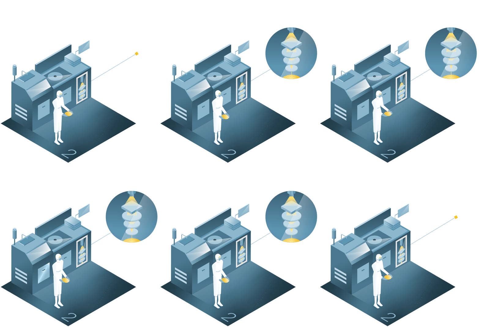
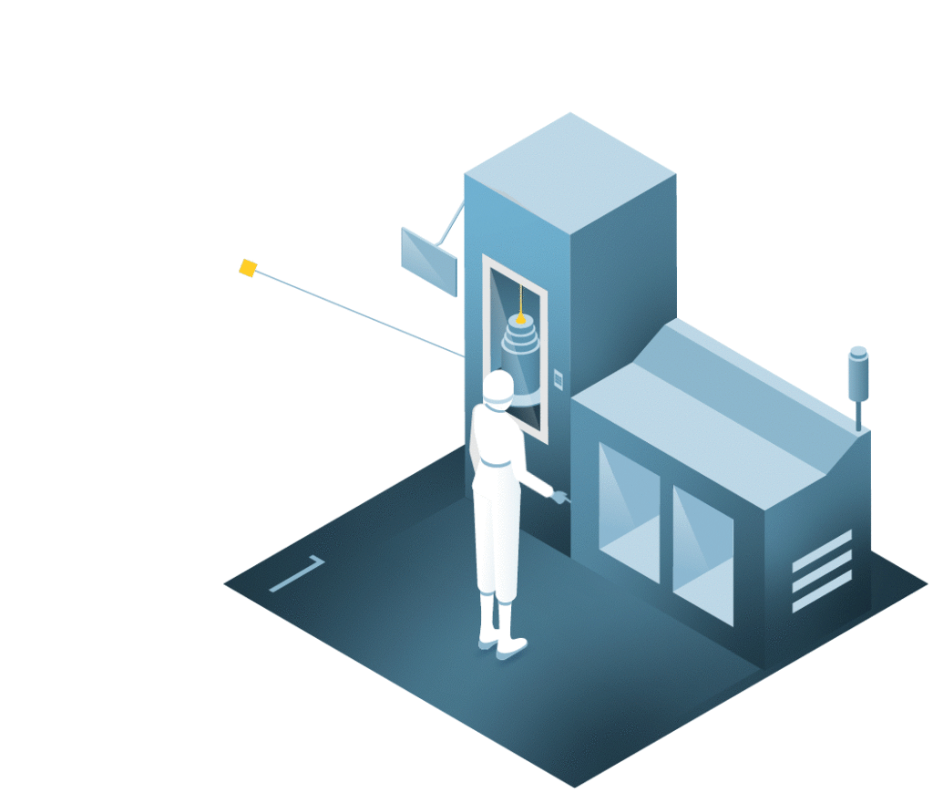
These guys built lenses smaller than a hair strand and stuck them directly on silicon chips. Instead of burning electricity to do AI math, they convert the numbers to light, bounce it through tiny lenses, and convert back to digital.
Here's why this matters: convolution operations eat 60-80% of the power in current AI chips. Your GPU burns 700 watts just moving electrons around to multiply numbers. Light doesn't give a shit about electrical resistance - it just goes through the lens and does the math for basically free.
Previous optical computing was lab demo bullshit with room-sized equipment and PhD students babysitting lasers. This uses standard 7nm CMOS processes - same fabrication lines TSMC runs for Apple's A-series chips.
Multiple Colors = Multiple Calculations at Once

They run red, green, and blue lasers through the same lens system simultaneously. Each color carries different data - same trick that lets fiber optic cables handle terabits per second.
Regular chips process AI layers one at a time, like a single-core processor from 1995. This thing processes multiple layers in parallel using different colored light. It's like having a GPU where each color wavelength is a separate compute unit.
Hit 98% accuracy on handwritten digits while using almost zero energy for the actual math. The power draw comes from the lasers and photodetectors, not the computation - so scaling up doesn't kill your electric bill.
The Good News: They Can Actually Make This Shit
![]()
Previous optical computing needed exotic materials and custom manufacturing. This uses the same CMOS process as regular chips. The lenses are just etched silicon - no weird external components, no retooling fabs.
They showed electron microscope photos of the actual working chips. Feature size is 100 nanometers, which is easy for current lithography. TSMC has been doing way smaller features for years.
The catch: scaling to real AI models needs thousands of these optical units per chip. Right now it's just a few lenses. You need 10,000+ perfect optical structures per die for serious workloads. That's where manufacturing yield will make or break the economics.
Where This Gets Fucked Up: Analog vs Digital Hell
The optical computation part works fine. The nightmare is connecting analog light systems to digital everything else. Light is analog - it drifts with temperature, wavelength variations, manufacturing tolerances. AI training needs precise digital numbers.
You're constantly converting between digital electrical signals and analog optical signals. Every conversion burns power and adds latency. Do that too much and you've lost your efficiency gains to the interface overhead.
The only way this works in production is hybrid: keep training digital, use optical for inference-only convolution where you can tolerate some accuracy loss. Pure optical AI is a pipe dream - mixed systems might actually work.
Will Anyone Actually Buy This?
Data center operators spend billions on electricity. If optical processing cuts even 50% of GPU power consumption, they'll throw money at it. Current GPUs burn 300-700 watts each, mostly on data movement and convolution operations.
But going from lab demo to production means handling models with 175B+ parameters, staying accurate when your data center hits 85°C, and making CUDA developers rewrite their software stacks. That's where most "revolutionary" chip technologies die a slow, expensive death.
Nvidia already uses optical interconnects in some systems, so the industry isn't allergic to hybrid designs. Question is whether this scales beyond handwritten digit recognition to actual transformer models and LLMs. Based on the math, it should work. Based on 20 years of optical computing promises, I'll believe it when data centers start buying chips.
