![]()
I spent three years debugging lithography systems that cost more than a skyscraper. When I heard ASML dropped €1.3 billion on Mistral AI, my first thought was "oh great, another consultancy deal that'll produce fancy dashboards nobody uses."
But then I remembered: ASML doesn't do stupid shit with their money. These are the people who charge $200M for a single machine and have customers lining up for years to buy them.
Why ASML's Machines Break Everything (Including Budgets)
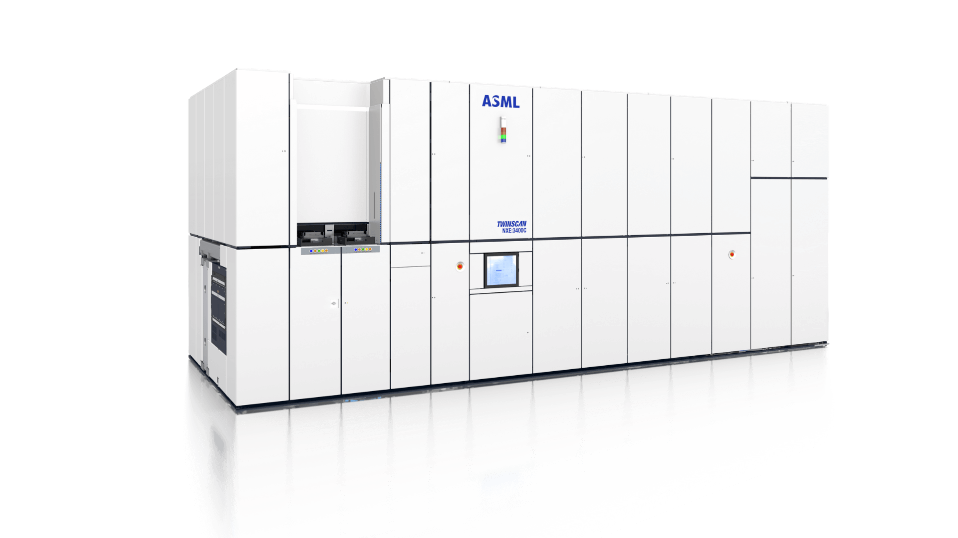
ASML has a monopoly on EUV lithography - the only way to make chips below 7nm. Their machines use 13.5nm wavelength light bounced off mirrors so perfect that if they were the size of Earth, the tallest mountain would be 6 feet.
I've watched a single speck of dust - literally one particle - shut down a $200M machine for 8 hours. The beam path has to be cleaner than deep space. The mirrors cost $20M each and if you breathe on them wrong, congratulations, you just bought ASML a new mirror.
When these things break, TSMC loses $1M per hour. I've seen engineers pull 72-hour shifts trying to get one back online because every minute of downtime pushes chip deliveries back weeks.
The control systems have something like 800+ sensors, maybe more - I stopped counting after the first few hundred. Focus accuracy needs to stay within maybe 2nm if you're lucky. Overlay precision can't drift more than about 1nm or you get systematic yield loss. One parameter goes out of spec and suddenly your $50M wafer lot is scrap.
Enter Mistral: Can AI Fix What Physics Broke?
Here's the thing - Mistral isn't building chatbots. They're training models that can actually parse sensor data and control systems. ASML's betting they can teach AI to predict when a $200M machine is about to shit the bed.
The dream scenario: Instead of me staring at hundreds of sensor readings trying to figure out why overlay accuracy went to hell, AI spots the pattern 2 hours before failure. Instead of trial-and-error parameter tuning that wastes $50K in test wafers, AI optimizes the recipe based on real-time process variations.
I've debugged enough focus/exposure matrix failures to know this could actually work. In my experience, the failure modes seem complex but they're not completely random - I started seeing patterns after debugging the same issues over and over. EUV dose variations and stochastic effects follow predictable curves. Resist line edge roughness patterns have telltale sensor signatures.
The question isn't whether patterns exist - it's whether AI can learn them fast enough to matter.
The Reality Check: Why This Could Fail Hard
Physics doesn't negotiate. EUV works by generating plasma hotter than the sun's surface, then using that to create 13.5nm light that gets bounced around mirrors in a vacuum. When something goes wrong, it's usually because quantum mechanics said "fuck you" to your control algorithm.
I've seen stochastic defects appear completely randomly despite perfect process control. You can't predict what doesn't follow patterns. Photon shot noise is literally quantum randomness - AI won't fix that.
Fab engineers trust nothing. I once watched a fab reject a software update because it changed the boot screen color. These people don't let you install Chrome without six months of qualification. You think they're gonna let AI control their $200M toys?
Training data costs millions. Each failed wafer run costs $100K+ in materials. You can't just run experiments to generate training data. ASML needs to train AI models on data from production runs that absolutely cannot fail. Catch-22: you need failures to learn from failures, but failures cost too much to generate.
Plus, each fab is different. Different suppliers, different processes, different contamination sources. An AI trained on TSMC data might be useless at Samsung.
But Maybe ASML Knows Something We Don't
They have a monopoly. When ASML says "our new machines have AI," customers don't get to say no. TSMC isn't switching to... who exactly? There is no alternative.
€1.3 billion buys real talent. Not consultants who learned TensorFlow last month. ASML can afford to hire the PhDs who actually understand both quantum optics and machine learning for manufacturing.
Fab yields are already hitting physics limits. Advanced node yields plateau around 70-80%. If AI can push that to 85%, it's worth tens of billions globally. The math works even if the AI only prevents one major downtime event per month.
ASML also has something most AI companies don't: 20 years of lithography data from thousands of machines. They know exactly which parameters correlate with failures. The machine learning problem is well-defined.
How to Tell if This is Real or Just Expensive Theater
I've seen enough "AI partnerships" that produced nothing but PowerPoint decks and invoices.
Red flags to watch for:
- Marketing whitepapers about "transformative AI solutions"
- Vague metrics like "improved operational efficiency"
- No actual data on critical dimension uniformity or overlay accuracy
Signs it's actually working:
- Published data showing measurable yield improvements
- Specific reductions in mean-time-to-repair
- Actual technical papers at SPIE Advanced Lithography, not just press releases
- Customer testimonials from TSMC or Samsung engineers, not marketing departments
Bottom line: €1.3 billion means ASML thinks AI can fix real problems, not generate better slide decks. We'll know in 18 months if Mistral can deliver or if this becomes another expensive lesson in why hardware is hard.
My bet? It'll work for narrow use cases - predicting mirror contamination, optimizing resist recipes, maybe catching some reticle defects early. But the "AI revolutionizes lithography" headlines are probably bullshit. Physics is still in charge.